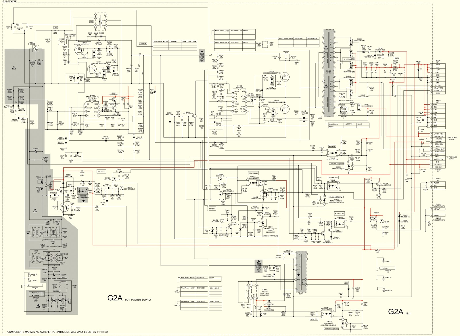
E3.schematic Schematic diagrams: sony kdl-40/46/t3500/40v2900 – smps schematic Sony kdl diagrams schematics magnify
JVC L-E3 Circuit Diagram
Schematics xperia schematic Electrical intelligently quickly bom Sony mobile schematics
E3.schematic
Jvc l-e3 circuit diagramE3.viewerplus Zuken topology.
.
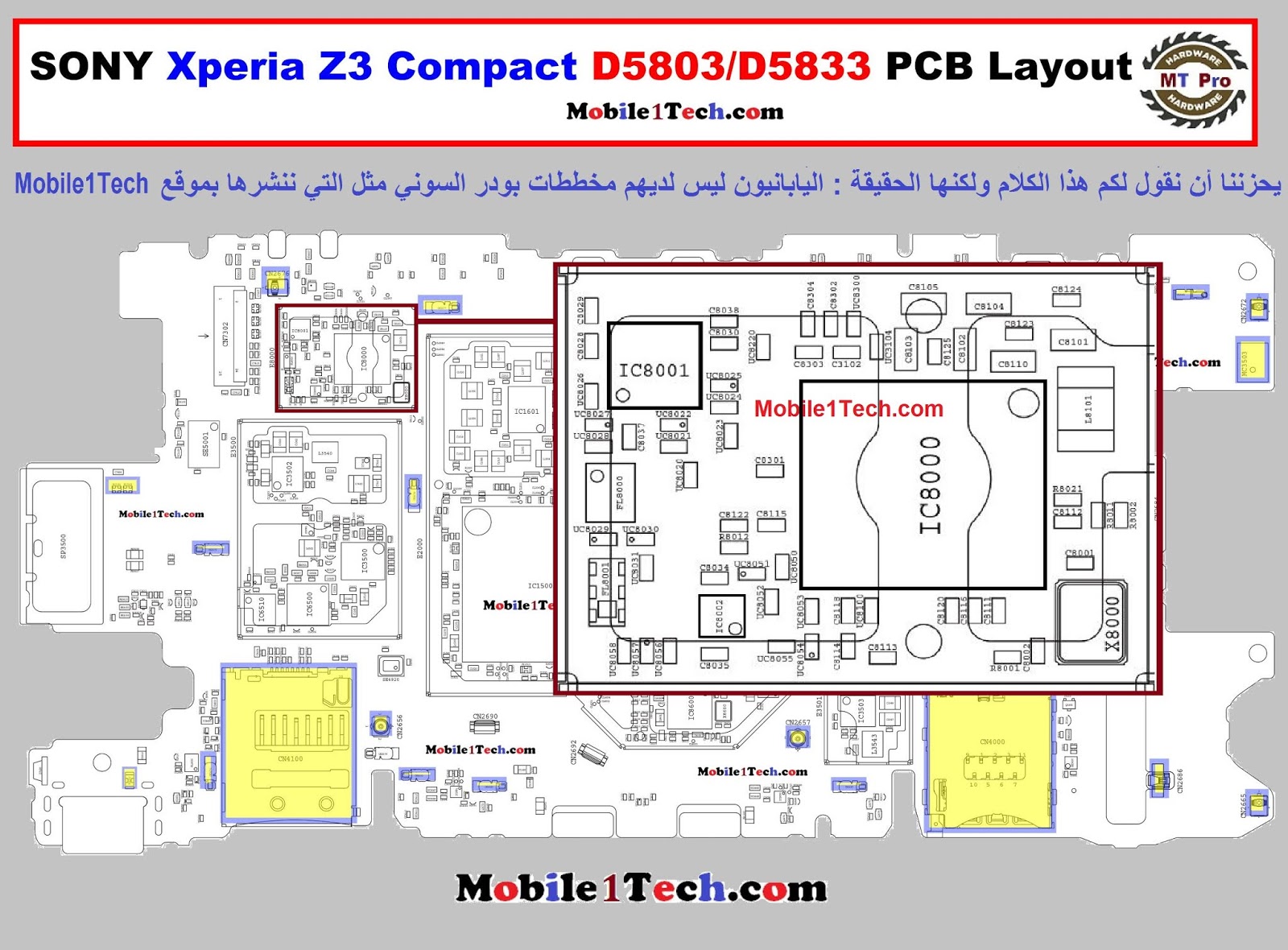
Sony Mobile Schematics

JVC L-E3 Circuit Diagram

E3.viewerPlus | Integration von Service und Produktion | Zuken GmbH

E3.Schematic - The Electrical Diagram Project Made Quickly and

E3.Schematic - The Electrical Diagram Project Made Quickly and
